
Author Affiliations
Abstract
1 State Key Laboratory of Artificial Microstructure and Mesoscopic Physics, School of Physics, Peking University, Beijing 100871, China
2 Beijing SinoGaN Semiconductor Technology Co., Ltd., Beijing 101399, China
3 Nano-optoelectronics Frontier Center of Ministry of Education, Peking University, Beijing 100871, China
4 Collaborative Innovation Center of Quantum Matter, Beijing 100871, China
The development of semiconductors is always accompanied by the progress in controllable doping techniques. Taking AlGaN-based ultraviolet (UV) emitters as an example, despite a peak wall-plug efficiency of 15.3% at the wavelength of 275 nm, there is still a huge gap in comparison with GaN-based visible light-emitting diodes (LEDs), mainly attributed to the inefficient doping of AlGaN with increase of the Al composition. First, p-doping of Al-rich AlGaN is a long-standing challenge and the low hole concentration seriously restricts the carrier injection efficiency. Although p-GaN cladding layers are widely adopted as a compromise, the high injection barrier of holes as well as the inevitable loss of light extraction cannot be neglected. While in terms of n-doping the main issue is the degradation of the electrical property when the Al composition exceeds 80%, resulting in a low electrical efficiency in sub-250 nm UV-LEDs. This review summarizes the recent advances and outlines the major challenges in the efficient doping of Al-rich AlGaN, meanwhile the corresponding approaches pursued to overcome the doping issues are discussed in detail.
AlGaN-based UV-LEDs Al-rich AlGaN doping Journal of Semiconductors
2024, 45(2): 021501
Author Affiliations
Abstract
1 State Key Laboratory of Artificial Microstructure and Mesoscopic Physics, School of Physics, Peking University, Beijing 100871, China
2 Frontiers Science Center for Nano-optoelectronics & Collaboration Innovation Center of Quantum Matter, Peking University, Beijing 100871, China
3 Suzhou Institute of Nano-Tech and Nano-Bionics (SINANO), Chinese Academy of Sciences, Suzhou 215123, China
4 International Center for Quantum Materials, Peking University, Beijing 100871, China
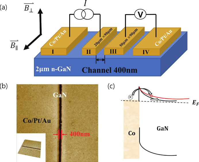
Spin injection and detection in bulk GaN were investigated by performing magnetotransport measurements at low temperatures. A non-local four-terminal lateral spin valve device was fabricated with Co/GaN Schottky contacts. The spin injection efficiency of 21% was achieved at 1.7 K. It was confirmed that the thin Schottky barrier formed between the heavily n-doped GaN and Co was conducive to the direct spin tunneling, by reducing the spin scattering relaxation through the interface states.
GaN spin injection Schottky barrier magnetoresistance Journal of Semiconductors
2023, 44(8): 082501
1 北京大学宽禁带半导体研究中心, 北京 100871
2 北京大学人工微结构和介观物理国家重点实验室, 北京 100871
3 教育部纳光电子前沿科学中心, 北京 100871
4 量子物质科学协同创新中心, 北京 100871
Si衬底因兼具大尺寸、低成本以及与现有CMOS工艺兼容等优势, 使Si衬底上GaN基射频(RF)电子材料和器件成为继功率电子器件之后下一个该领域关注的焦点。由于力学性质与低阻Si衬底不同, 高阻Si衬底上GaN基外延材料生长的应力控制和位错抑制问题仍然困难, 且严重的射频损耗问题限制着其在射频电子领域的应用。本文简要介绍了Si衬底上GaN基射频电子材料的研究现状和面临的挑战, 重点介绍了北京大学研究团队在高阻Si衬底上GaN基材料射频损耗的产生机理, 以及低位错密度、低射频损耗GaN的外延生长等方面的主要研究进展。最后对Si衬底上GaN基射频电子材料和器件的未来发展作了展望。
Si衬底上GaN 金属有机化合物化学气相沉积 应力 位错 射频损耗 GaN-on-Si MOCVD stress dislocation RF loss
1 贵州大学空间结构研究中心, 贵阳 550025
2 贵州大学, 贵州省结构工程重点实验室, 贵阳 550025
为研究石灰石粉(以下简称石粉)参数对水泥水化热的影响, 利用TAM Air-八通道微量热仪探究不同石粉含量和粒径对水泥水化放热量以及水化放热速率的影响。研究表明, 随着石粉含量的增加, 辅助胶凝材料的水化放热量和水化放热速率总体上呈降低的趋势。其中当石粉含量为15%(质量分数)时, 石粉粒径为400目时放热量为223.22 J/g, 水化峰值速率为2.399 2 mW/g, 石粉粒径为3 000目时放热量为215.98 J/g, 水化峰值速率为2.214 0 mW/g, 其放热量和水化峰值速率降低的趋势最明显。同时, 当石粉掺量较大时, 石粉粒径对水化反应的影响更加明显, 粒径过小或者过大都会提高水化放热量和水化放热速率。当石粉粒径为1 250目时水化放热量较小且水化放热速率较低。通过物相分析发现, 石粉的加入不会使体系产生新物质, 当石粉含量为15%(质量分数)、粒径为1 250目时, Ca(OH)2衍射峰强度最高并伴随着大量C-S-H的生成, 说明了该组石粉能够更大程度地促进水泥水化, 使反应更充分。
石灰石粉 胶凝材料 粒径 掺量 水化热 物相分析 limestone powder cementitious material particle size content hydration heat phase analysis
1 北京大学宽禁带半导体研究中心,北京 100871
2 北京大学人工微结构和介观物理国家重点实验室,北京 100871
3 北京大学物理学院,北京 100871
4 量子物质科学协同创新中心,北京 100871
5 教育部纳光电子前沿科学中心,北京 100871
以氮化镓(GaN)、AlN(氮化铝)为代表的Ⅲ族氮化物宽禁带半导体是研制短波长光电子器件和高频、高功率电子器件的核心材料体系。由于缺少高质量、低成本的同质GaN和AlN衬底,氮化物半导体主要通过异质外延,特别是大失配异质外延来制备。由此导致的高缺陷密度、残余应力成为当前深紫外发光器件、功率电子器件等氮化物半导体器件发展的主要瓶颈,严重影响了材料和器件性能的提升。本文简要介绍了氮化物半导体金属有机化学气相沉积(MOCVD)大失配异质外延的发展历史,重点介绍了北京大学在蓝宝石衬底上AlN、高Al组分AlGaN的MOCVD外延生长和p型掺杂、Si衬底上GaN薄膜及其异质结构的外延生长和缺陷控制等方面的主要研究进展。最后对Ⅲ族氮化物宽禁带半导体MOCVD大失配异质外延的未来发展做了简要展望。
氮化镓 氮化铝 金属有机化学气相沉积(MOCVD) 大失配异质外延 宽禁带半导体 GaN AlN metal organic chemical vapor deposition (MOCVD) large latticemismatched heteroepitaxial growth wide bandgap semiconductor
1 湖北科技学院 电子与信息工程学院, 湖北 咸宁 437100
2 华中科技大学 武汉光电国家研究中心, 湖北 武汉 430074
双色激光脉冲激励气体等离子体产生太赫兹波是得到高强度宽频带太赫兹波的重要方法, 本文利用光电流模型研究了该方法中激光能量对产生太赫兹波的影响。理论计算表明, 太赫兹波随激光能量的增大而增强, 而太赫兹波的频谱结构不受激光能量的影响。分析了双色激光能量影响太赫兹波强度的原因, 并利用自由电子浓度和电子电流密度诠释了该影响的内在物理机制。该研究为提高太赫兹辐射强度提供了一种有效的途径。
飞秒激光脉冲 太赫兹波 气体等离子体 光电流模型 femtosecond laser pulse terahertz wave gas plasma photocurrent model
当高强度短/超短脉冲激光聚焦于靶材表面或介质内部时,若其峰值功率密度超过某一阈值,靶材表面或介质内部会形成等离子体,等离子体与工件相互作用进行材料去除,这一过程称为激光诱导等离子体微加工(LIPMM)。这一加工技术可以高效吸收激光能量,具有损伤小、效率高、应用广等特点,已被广泛应用于微加工领域。为此介绍了LIPMM的微加工原理,进一步阐述了以固体为靶材和以液体为介质的LIPMM的研究进展,对LIPMM未来所面对的问题和发展方向进行了总结和展望。
激光光学 微加工 短/超短脉冲激光 激光诱导等离子体微加工 激光与光电子学进展
2020, 57(11): 111405

Author Affiliations
Abstract
1 School of Physics, State Key Laboratory for Mesoscopic Physics, Academy for Advanced Interdisciplinary Studies, and Nano-optoelectronics Frontier Center of Ministry of Education, Peking University, Beijing 100871, China
2 Key Laboratory of Photochemical Conversion and Optoelectronic Materials, Technical Institute of Physics and Chemistry, Chinese Academy of Sciences, Beijing 100190, China
3 State Key Laboratory of Precision Measurement Technology and Instruments, Department of Precision Instruments, Tsinghua University, Beijing 100084, China
4 Collaborative Innovation Center of Quantum Matter, Beijing, China
With the recent development of the metasurface, generating an optical vortex in optical far or near fields is realized in various ways. However, to generate vortices in both the near and far fields simultaneously is still a challenge, which has great potential in the future compact and versatile photonic system. Here, a bi-channel optical vortex generator in both the near and far fields is proposed and demonstrated within a single metasurface, where the surface plasmon vortex and the far-field optical vortex can be simultaneously generated under circularly polarized light. The ability of generating vortices with arbitrary topological charges is experimentally demonstrated, which agrees well with simulations. This approach provides great freedom to integrate different vortex generators in a single device, and offers new opportunities for integrated optical communications, trapping, and other related fields.
Photonics Research
2020, 8(6): 06000986
Author Affiliations
Abstract
1 Institute of Physics, Otto-von-Guericke-University Magdeburg, 39106 Magdeburg, Germany
2 State Key Laboratory for Mesoscopic Physics and Frontiers Science Center for Nano-optoelectronics, School of Physics, Peking University, Beijing 100871, China
3 Department of Electrical and Electronic Engineering, Mie University, Mie 514-8507, Japan
4 Advanced Micro-Fabrication Equipment Inc., Shanghai 201201, China
5 Collaborative Innovation Center of Quantum Matter, Peking University, Beijing 100871, China
6 e-mail: Gordon.Schmidt@ovgu.de
7 e-mail: wangshi@pku.edu.cn
Investigating closely stacked GaN/AlN multiple quantum wells (MQWs) by means of cathodoluminescence spectroscopy directly performed in a scanning transmission electron microscope, we have reached an ultimate spatial resolution of . The pseudomorphically grown MQWs with high interface quality emit in the deep ultraviolet spectral range. Demonstrating the capability of resolving the 10.8 nm separated, ultra-thin quantum wells, a cathodoluminescence profile was taken across individual ones. Applying a diffusion model of excitons generated by a Gaussian-broadened electron probe, the spatial resolution of cathodoluminescence down to the free exciton Bohr radius scale has been determined.
Photonics Research
2020, 8(4): 04000610
1 吉林大学基础医学院细胞生物学系, 吉林 长春 130021
2 吉林大学集成光电子学国家重点实验室,电子科学与工程学院, 吉林 长春 130012
3 吉林大学第一医院放疗科, 吉林 长春 130021
稀土掺杂的上转换纳米发光材料(UCNP)可以将低频光子转化为高频光子,通常是近红外光激发,可见光发射,这个独特的光学性质使其具有良好的生物学应用前景。近年来,UCNP已经在成像、传感等领域取得了重要进展,本文对近年来UCNP的合成、表面修饰以及在生物检测等方面的应用进行综述,涵盖了生物检测方面的重要进展,包括基于上转换荧光的温度、离子、小分子以及生物体内的重要蛋白与核酸等检测应用。
生物光学 稀土发光 上转换发光 荧光探针 生物传感


